Wafer Production
Semiconductor
Capteura® Parallelism Measurement Systems typically contains 3 to 6 displacement sensors connected to a full range of amplifiers driven by a wide range of applications with specific measurement requirements. Parallelism is most commonly called out as surface parallelism. Some examples:
Semiconductor Wafer Production
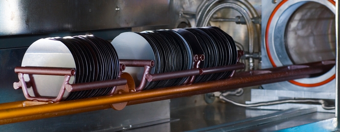
Semiconductor wafer production involves the sequential deposition of various materials onto the silicon wafer substrate in order to achieve the electrical characteristics specified by the semiconductor device customer. The entire deposition process takes place within a vacuum chamber in order to eliminate contamination and to control parameters. The deposition process utilizes a wafer holder plate where sequential layers of material are deposited onto the silicon wafer. In order to achieve uniform thickness of the deposited layers at the time that the deposition occurs, the parallelism of the wafer holder plate relative to the deposition plate must be confirmed through precise measurement.
A 3-point non contact tool is proportionally sized to accommodate a 300mm process or 200mm process. Custom designed tools is a Capacitec specialty. We work with our customers closely to design and build OEM quality measurement tools.
Additional Semiconductor Applications
- Grinding silicon wafer to a known thickness using a 3-point sensor connected to a Gapmaster 3 instrumentation to measure the height of the wafer grinding station to groom to the nominal thickness. Link to parallelism
- Additional custom OEM dimension set up tools available for the semiconductor industry